JVX6200iRF
JVX6200iRF In-line X-ray metrology platform for FEOL, MEOL & BEOL for the semiconductors industry
JVX6200iRF features a multi channel metrology platform with small spot XRF and Fast XRR channels ,for measurement of thin metal layer stacks on product or blanket wafers.The tool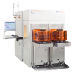 is designed for advanced process control of metals and transparent films at the back-end of line (BEOL), MEOL and front end of line (FEOL) of advanced semiconductors processes (Logic, DRAM, Flash and HDD process lines).
XRR (X-Ray Reflectometry) Thickness, Density & Roughness of ultra-thin metal and dielectric films with thickness as low as 8Å for the FEOL, MEOL and BEOL:
- XRR channel: first principle, no calibration needed.
- Fast, small spot XRR channel for blanket or patterned wafers.
XRF (X-Ray Fluorescence) Thickness, elemental analysis and composition of thin and thick metal layers for the FEOL, BEOL and WLP:
- High brightness XRF source with high efficiency detector Si(Li) for heavy metals (Sn, Ag etc)
- Advanced XRF algorithms for fast and accurate measurement and calibration (FP)
The JVX 6200iRF is a dual channel tool with Fast convergent beam XRR and vertical illumination XRF channel. Combination of the two channels enables utilization of the tool for various applications. The nEXT operating software includes fully automated recipe driven measurements and FP analysis.
XRF: Measure on product (<50µm pads) or blanket wafers
- Ti and TiN
- W plug and WSi
- Cu: CMP (pre and post)
- UBM and RDL multi layer analysis (Au, Cu, Ni, Pd, Ti )
- Bumps and µ-bumps: Sn-Pb, Sn-Ag
XRR: Measure on scribe line or blanket wafers
- HKMG :Complex metal gate stacks (e.g. Si//SiO2/HfO2/TiN/TaN/TiN)
- Cu/Ta Seed/Barrier • Ti/TiN • Silicides NiSix, CoSix , WSix
- SiON
- ONO
- ACL (Amorphous Carbon Layer) & DLC (Diamond like Carbon)
- ZAZ
- XRF: Vertical illumination/detection geometry with polycapillary optics for small spot (20µm FWHM)
- XRR: Fast convergent beam: Flash mode, no moving parts
JVX6200i Platform:
- Non destructive, production proven
- Fully 300/200mm fab automated, for high volume
- E84, EHT, SEC/GEM automation
- Certifications: S2/S8, CE, ISO9001, ISO14001, ISO18001
XRF
- Normal incidence micro spot XRF
- FWHM of <20µm, no dependence on height variation
- Si(Li) detectors , efficient for high energy photos
- Multiple detectors allow photon collection from a large solid angle, giving high throughput
- Superior efficiency for high energies (Such as AgKα and SnKα )
- Fully automated recipe driven measurements
XRR
- Convergent beam, small spot control for scribe line, small pad measurement capability
- Measurements of optically opaque and transparent layers
- Thickness, Density and layer roughness. Single layer or complex stacks (stack analysis)
- Sub-Angstrom precision & accuracy
- Sub Angstrom Tool matching
- Fully automated recipe driven measurements
