|
 The QC3 is the latest model in the long-established and well-proven QC range of High Resolution X-ray diffractometers, with over a 20-year pedigree, and hundreds in use around the world in compound semiconductor and silicon-germanium research and manufacturing facilities. It is a high resolution X-ray diffraction tool that is ideal for semiconductor development and quality control. It is used for the measurement of composition and thickness in epitaxial layers of almost any material. The system uses standard sealed tube optics, combined with a variety of beam conditioning crystals that can be optimized to give the highest combination of resolution and intensity for each application. The QC3 offers true automated operation, with straight-forward horizontal sample mounting, and fully automated alignment, measurements, and data analysis. Data analysis can be performed automatically, or offline using our popular RADS software. The sample stage has a full 300mm of travel, allowing for measurements of large wafers, or several smaller wafers simultaneously. An optional robot handler is available for automated loading and measurement from cassette. It is the ideal tool for routine analysis of semiconductor substrates, epilayer structures and processed device wafers for all compound semiconductor materials. The QC3 is the latest model in the long-established and well-proven QC range of High Resolution X-ray diffractometers, with over a 20-year pedigree, and hundreds in use around the world in compound semiconductor and silicon-germanium research and manufacturing facilities. It is a high resolution X-ray diffraction tool that is ideal for semiconductor development and quality control. It is used for the measurement of composition and thickness in epitaxial layers of almost any material. The system uses standard sealed tube optics, combined with a variety of beam conditioning crystals that can be optimized to give the highest combination of resolution and intensity for each application. The QC3 offers true automated operation, with straight-forward horizontal sample mounting, and fully automated alignment, measurements, and data analysis. Data analysis can be performed automatically, or offline using our popular RADS software. The sample stage has a full 300mm of travel, allowing for measurements of large wafers, or several smaller wafers simultaneously. An optional robot handler is available for automated loading and measurement from cassette. It is the ideal tool for routine analysis of semiconductor substrates, epilayer structures and processed device wafers for all compound semiconductor materials.
Tool brochures can be found here. Related application notes can be found here.
- Dedicated and optimized HRXRD system with no compromise required to accommodate other techniques
- High intensity gives either higher precision for the same throughput or higher throughput for same precision (compared to previous QC systems)
- Low cost of ownership
- User friendly system
- Low running costs
- Batch wafer measurements either with a robot or multiple samples loaded
- No expert required to run the system
- Fully automated alignment, measurement and analysis of wafers
- Uses established RADS analysis software for either automated or off-line analysis
- Results can be reported remotely
The QC3 is suitable for most semiconductor-based structures and device structures, including, but not limited to: - GaN-based LEDs and laser structures
- III-V, II-VI and IV-IV based materials (HEMTs, HBTs...)
- Si based materials
- SiGe-based HBT structures
- Single and multilayer epitaxial films
- MQW structures
- Superlattice structures
General- Compact, high-resolution diffractometer
- Horizontal specimen mounting on detachable holders - up to 300mm sample size
- Full 300mm scanning capability with sample plates with multiple wafer locations
- Pre-aligned beam conditioners available for materials with low dislocation content, such as GaAs, InP, and Si based compounds, and materials with higher defect densities, such as GaN and ZnO.
- EDRc Dynamic Range X-ray detector
- Triple Axis option available
- Robot loading option available
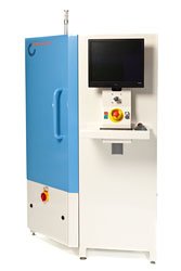
Enclosure- Fully contained within a free-standing steel enclosure
- Easy sample access
- Full X-ray safety interlocks, fail-safe shutter and warning lamps
- Size (approx): 1m x 1m
|


